Printed Circuit Boards – Overview and Explanation
Printed Circuit Boards
- A printed circuit board is an electrical circuit used to mechanically support electronic components and to connect them electrically using conductive tracks. The term PCB is used as an abbreviation for the printed circuit board. It’s important to note the difference between a blank PCB and a PCB with components. A blank PCB is a plate without any soldered components, whereas a PCB with components has various resistors, capacitors, connectors, ICs, etc. mounted on its surface.
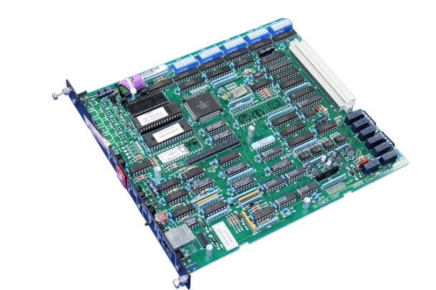
Figure 1: Printed Circuit Board with Components
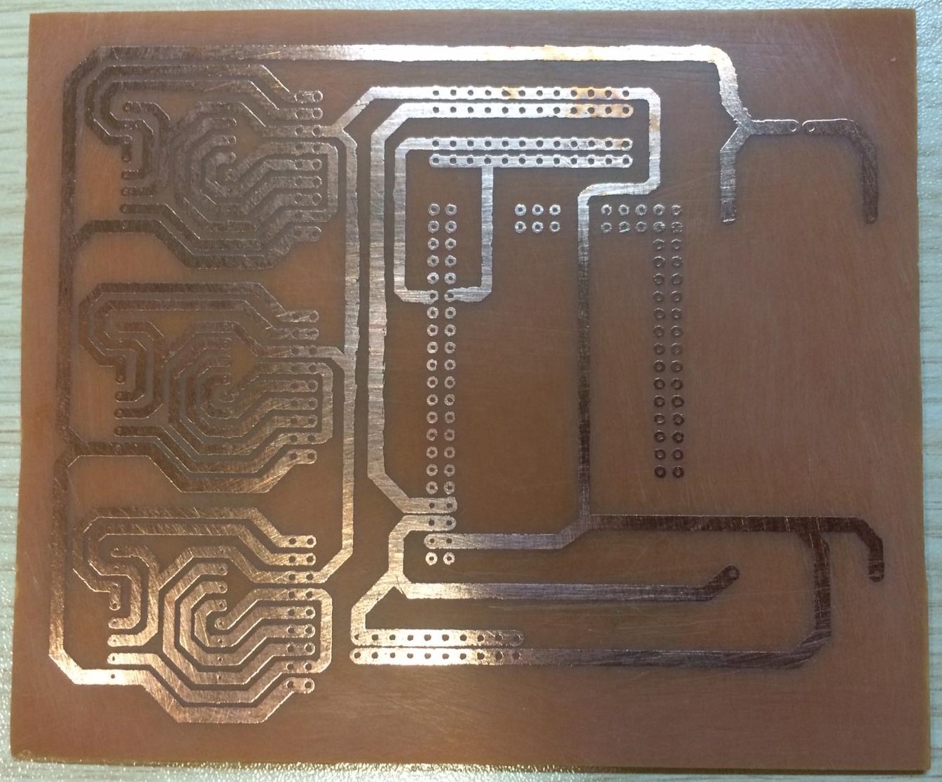
Figure 2: Blank Printed Circuit Board
- All the electronic components are either connected to the PCB or assembled by soldering. If the PCB had not been invented, all components would be connected by a large number of wires, which would reduce the reliability of circuits and increase the complexity of the design. Fortunately, printed circuit boards have been used for a long time, as they provide structure and organization for tons of electronic components to be mounted on their surface. PCBs can be easily customized for any application using computer-aided design (CAD) and manufacturing (CAM) software. This software helps electrical engineers design models of PCBs on the computer first before actually building the circuit itself.
- As you can tell, printed circuit boards (PCBs) are extremely common and are one of the essential blocks of modern electronic equipment.
Types of Printed Circuit Boards
- Nowadays, a modern computer printed circuit board looks like a multilayer labyrinth of hundreds of copper wires. Due to the mature printed circuit board manufacturing technology, PCBs have a variety of chemical and mechanical properties. So, it is really important to have an adequate understanding of how PCBs are made and what the main features are.
- Several types of printed circuit boards are available for circuit design. Printed circuit boards are traditionally classified according to their physical and chemical properties. PCBs are manufactured in one, two, or multi-layers depending on the complexity of the circuit. Although there are various types of printed circuit boards for customers, the most popular are the four main PCB types shown in Figure 3.
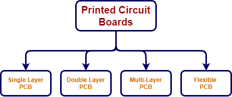
Figure 3: Printed Circuit Board
- Single Layer PCB is a low-cost printed circuit board that has only a single conductive layer above the substrate.
- Double Layer PCB has an FR4 substrate layer between two conductive layers. Since through-hole electronic components and surface mount (SMD) components can be soldered on both sides of this type of PCB, the solder mask is applied to both sides of the printed circuit board.
- Multi-layer PCB is a printed circuit board with more than two conductive layers. This type of printed circuit board should have a minimum of three conductive layers. All conductive layers are interconnected by copper-plated holes. This type of PCB is commonly used in computer motherboards.
- A flexible PCB is an easily bent printed circuit board. It saves considerable amounts of space compared to a regular rigid printed circuit board. Flexible PCBs can be produced as single, double, or multi-layer. They are often used in solar panels and smartwatches.
Construction of the Printed Circuit Board
- There are several different types of materials that are used to manufacture printed circuit boards. The materials, substrates, chemical properties, and construction are based on the type of circuit that’s being designed and its application.
- PCBs are categorized in terms of their heat resistance by the term called FR which means flame retardant. There are several types of flame-retardant (FR) printed circuit boards, however, the FR4 type is the most popular choice. FR4 is a composite material composed of woven fiberglass fabric with flame-resistant epoxy resin binders. FR4 is very popular due to its better stability with differences in temperature compared to other flame-retardant substrates. It is also easier to place FR4 between the conductive layers in the PCB.
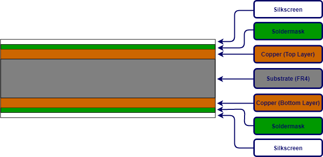
Figure 4: Construction of the Double Layer Printed Circuit Board
- Fıgure 4 is a diagram of how a double-layer PCB is constructed using an FR4 substrate. As you can see two conductive (copper) sheets cover the (non-conductive dielectric) substrate. All components are mounted on the (copper) upper and lower layers of the printed circuit board.
- There is another layer on the copper layer called the solder mask. This layer can be recognized commonly by its unique green color, but also it can be in any other color. A solder mask is used as an insulating layer to prevent unwanted contact of copper traces with other conductive materials on the PCB.
- The silkscreen is an additional layer on top of the solder mask layer that is used to print text, lines, or any shape on the surface of the printed circuit board. Epoxy ink is generally used for the screen printing process. The silkscreen layer can be used on the top and/or bottom layer of the printed circuit board according to user needs.
Contact Us
Accepted Payments